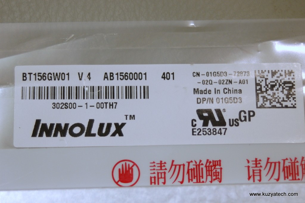
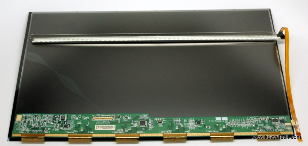
I’ve always wanted to see what the latest LCD panels look like inside, and such a chance just presented itself. I got my hands on a broken 15.6″ panel, used in many laptops these days. This particuar one had DP/N number on it, so I assume it was used in a Dell. Let us see how much we can learn looking at the design with limited access to device datasheets.
Original specs are:
- 1366X768 wide format
- LVDS interface
- LED backlight
The panel glass was cracked, so we can proceed with clear conscience,
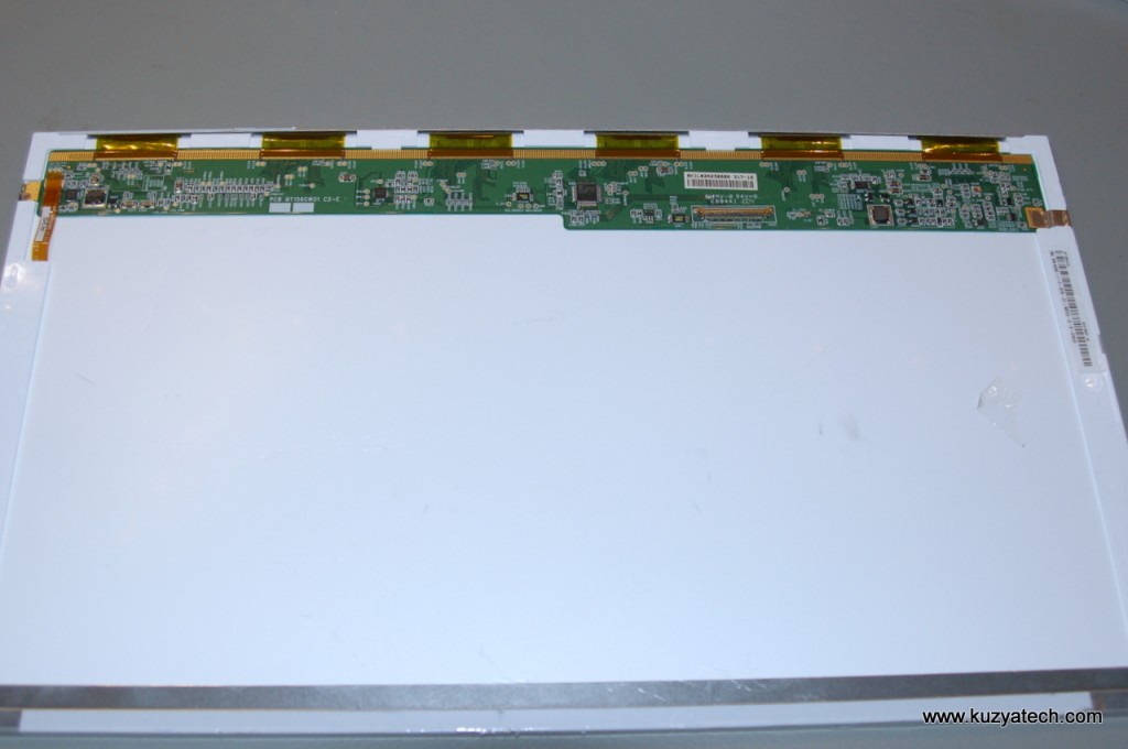
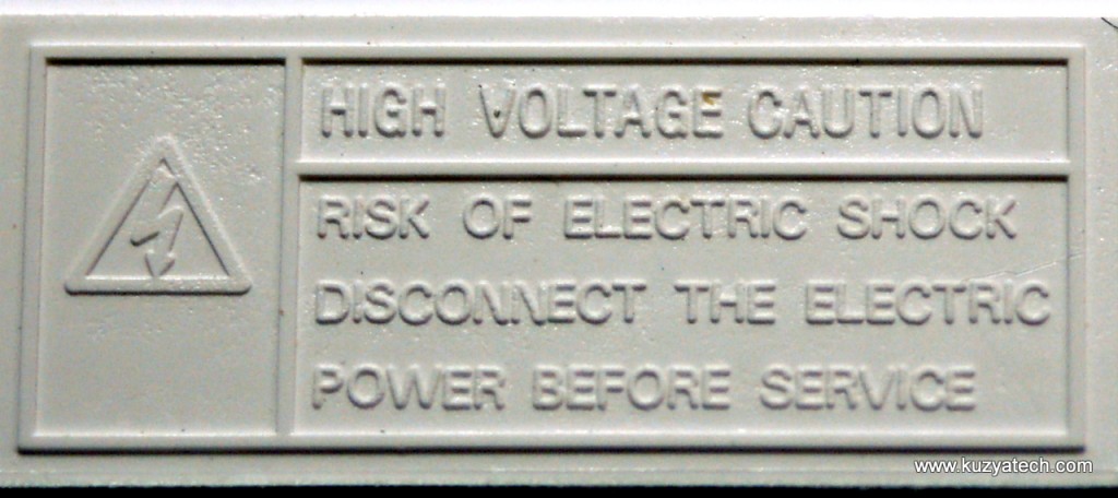
Driver board. Under the "Do not touch" label are six heatbonded flexes, each one with a bare driver die attached
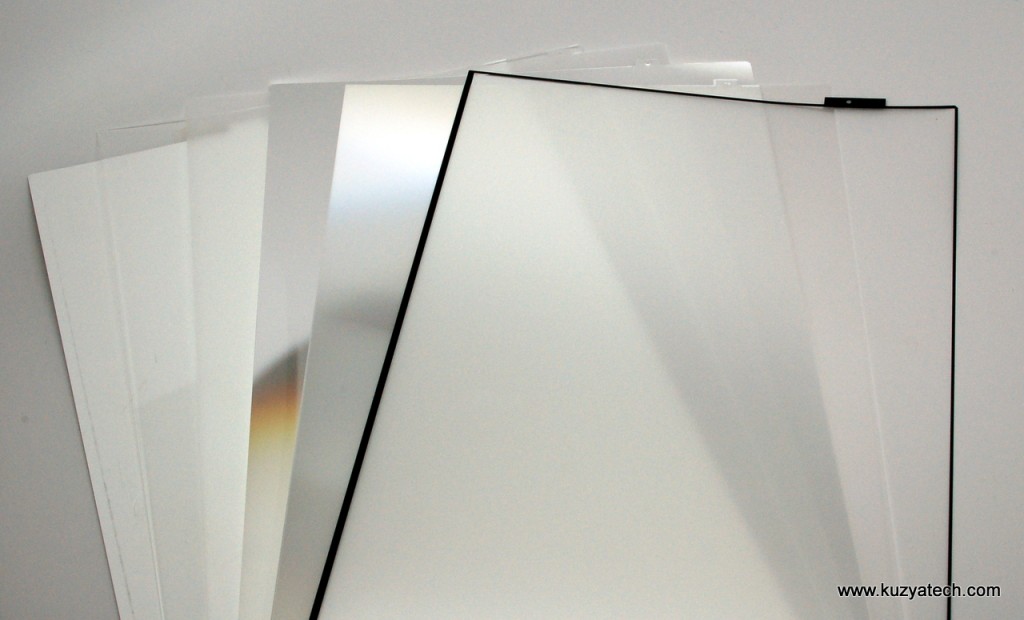
Optical films. Left to right- reflector, backlight sheet, diffuser, two layers that look like Fresnel lenses but could also be prism layers and another diffuser. All these were behind the panel.
Now on to the electronics. Most silicon that is labeled is from Novatek, a fabless company from Taiwan. No datasheets were to be found during my brief web search, so I’ll have to deduce functionality from what I see on the board. Feel free to correct!
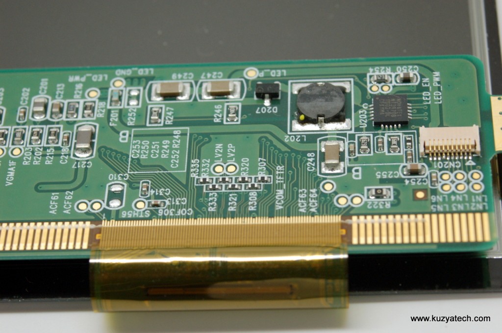
Backlight looks to be a pretty typical boost configuration with six LED strings grounded through the switches in the driver and one common power rail. Enable and PWM input signals are nicely labeled, so there is still a possibility of driving the backlight standalone.
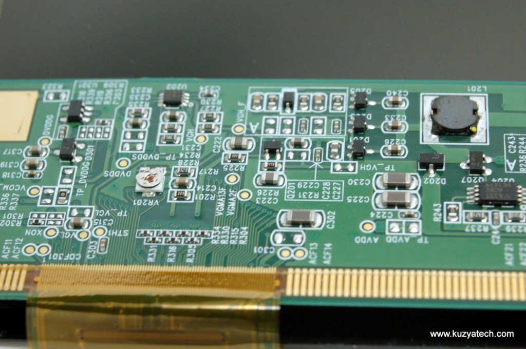
The chip is labeled 8333 (made by Seiko Instruments Inc) and is generating multiple voltages for the display. The three caps from L201 going to three diodes are parts of the charge pumps producing positive and negative voltages needed by the panel. (Usually +21,-9,+7 V etc). Input signals come through a 40 pin connector, with four differential pairs running LVDS.
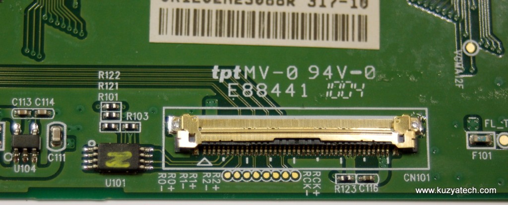
Looks like the connector is carrying (Right to left) Power, GND, 4 diff pairs of LVDS data and what appears to be I2C data to serial EEPROM. The top of the chip has S24C on it and the let side pins are all grounded- typical pinout for an I2C eeprom, where pins 1-3 are address and 4 is GND. Only puzzling part is power pin 8 that seems to go to the connector instead of power plane, and lack any decoupling caps. The EEPROM stores the so called EDID data for display identification to the main system. Regular monitors do the same via signals in the VGA cable.
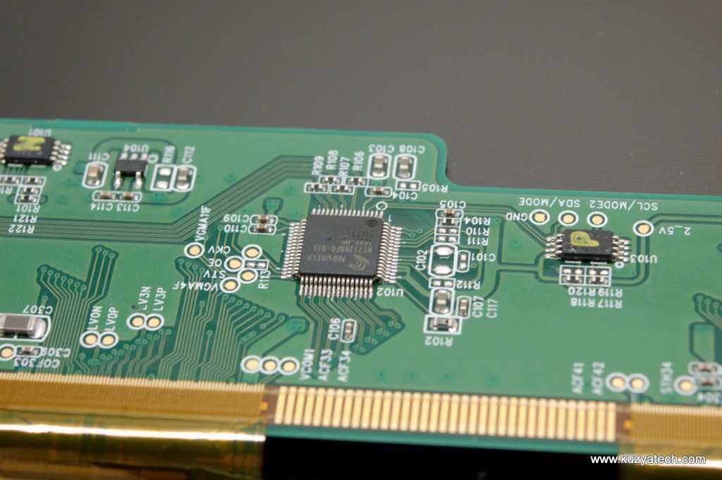
This chip U102 receives the four LVDS pair on one end and then outputs seven (CLK,LV0-LV5) that go across the board. They are then connected to the six panel drivers. U103 is another I2C eeprom storing chip’s configuration. U104 is looking like an LDO- the two large caps and a big trace on the back going to several other places on the board are a giveaway of that. Most likely it’s producing the 2.5V rail for the LVDS chip.
And now let us try recreating main connector pinout:
1 NC, 2-3 VCC (3.3V), 4 EEPROM VCC, 5 NC, 6 CLK_EDID, 7 DATA_EDID, 8-9 R0, 10 GND, 11-12 R1, 13 GND, 14-15 R2, 16 GND, 17-18 RCK, 19-30 NC, 31-33 GND, 34 NC, 35 LED_PWM, 36 LED_EN, 37 NC, 38-40 Backlight power supply (5V?)
This seems pretty similar to a lot of other panels, though some of the NCs are grounded on those.
Update 8/5/2012: thanks to the folks at the EEVblog Forum thread for a lot of insight on how these things work, and their help locating information on some of the parts and the display datasheet (older rev, but very close)


Can you or someone you know, supply me with the back light sheets kit for a MacBook Air A1369 mid 2011 ?
Sorry, no idea
can i buy just the optical film from you guys?
How can you find out the week code from the sn# on the panel ?
Im trying to find out the manufacturer date of my lnnolux panel from the sn#.
please help ….